I’m not an expert, but ASML uses a very powerful ultraviolet ‘cannon’ to edge patterns into their layers https://wikiless.northboot.xyz/wiki/Extreme_ultraviolet_lithography, and apparently (from the few lines of article txt) the Chinese are going for particle accelerators for edging instead. I wonder if they will use a beam or just fire away on a masked wafer.
Slightly ot, I think hybrid photonic computing is the future, but that would probably also benefit from smaller construction techniques, so …go go China.
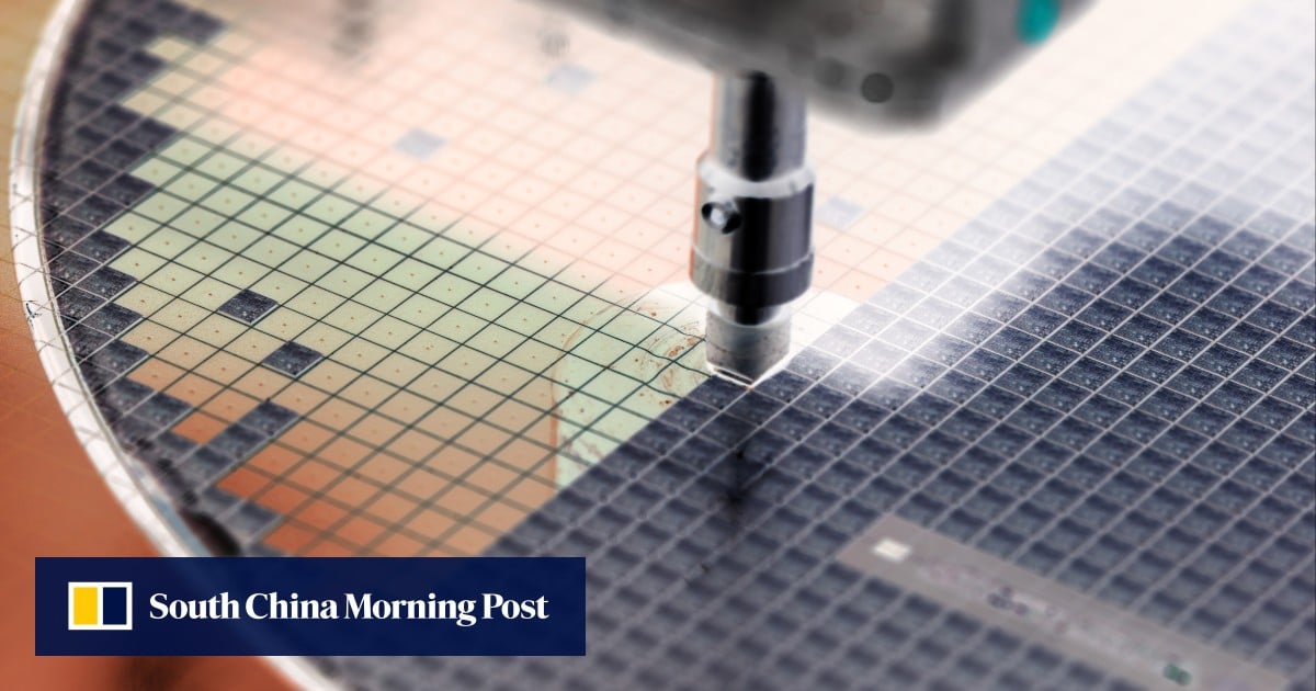
Compared with current ASML EUV technology, SSMB is a more ideal light source. It has a higher average power and higher chip production output with lower unit cost.
ASML creates an EUV source from laser-produced plasma, where strong laser pulses are projected to liquid microdroplets of tin. The laser crushes the droplets and produces EUV pulse light during the impact. After complex filtering and focusing, an EUV light source with a power of about 250W is produced.
Before reaching the chip, the EUV beam undergoes reflection from 11 mirrors, each causing about a 30 per cent energy loss. As a result, the power of the beam is less than 5W when reaching the wafer. This can become an issue when manufacturing turns to 3nm or 2nm.
SSMB technology avoids such concerns. SSMB beams achieve a higher output power of 1000W, and due to its narrow bandwidth, fewer reflecting mirrors are needed, which naturally generates higher terminal power.
I do think there is a lot of potential for alternative computing substrates like photonics or graphene.
This kind of stuff could end up being like going from vacuum tubes to transistors. We’re pushing the limits of what’s physically possible with silicon now, but even a crude alternative substrate could naturally afford far better performance, and then could be optimized for decades on end.


Unfortunately it was paywalled.
I’m not an expert, but ASML uses a very powerful ultraviolet ‘cannon’ to edge patterns into their layers https://wikiless.northboot.xyz/wiki/Extreme_ultraviolet_lithography, and apparently (from the few lines of article txt) the Chinese are going for particle accelerators for edging instead. I wonder if they will use a beam or just fire away on a masked wafer.
Slightly ot, I think hybrid photonic computing is the future, but that would probably also benefit from smaller construction techniques, so …go go China.
If someone is interested in chip construction and new AI trends in that area, I can recommend ‘Asianometry’ https://www.youtube.com/channel/UC1LpsuAUaKoMzzJSEt5WImw / https://redirect.invidious.io/channel/UC1LpsuAUaKoMzzJSEt5WImw and especially ‘Anastacia in tech’ https://www.youtube.com/channel/UCORX3Cl7ByidjEgzSCgv9Yw / https://redirect.invidious.io/channel/UCORX3Cl7ByidjEgzSCgv9Yw
They have not reported on this Chinese particle thing yet, tho…
here’s an archived version https://archive.ph/NrC6B
it does mention the advantages over ASML approach
I do think there is a lot of potential for alternative computing substrates like photonics or graphene.
Incidentally, there was a breakthrough fabricating 12-inch wafers with MoS2 which has potential to be a much faster substrate than silicon https://www.sciencedirect.com/science/article/abs/pii/S2095927323004206
This kind of stuff could end up being like going from vacuum tubes to transistors. We’re pushing the limits of what’s physically possible with silicon now, but even a crude alternative substrate could naturally afford far better performance, and then could be optimized for decades on end.
Damn, things are moving fast atmo ! Thx for info!
Here is an alternative Piped link(s):
https://www.piped.video/channel/UC1LpsuAUaKoMzzJSEt5WImw
https://www.piped.video/channel/UCORX3Cl7ByidjEgzSCgv9Yw
Piped is a privacy-respecting open-source alternative frontend to YouTube.
I’m open-source; check me out at GitHub.